Logic Analyzer Extensions


OVERVIEW
Record Digital and Analog Signals and Correlate Them to Program Flow
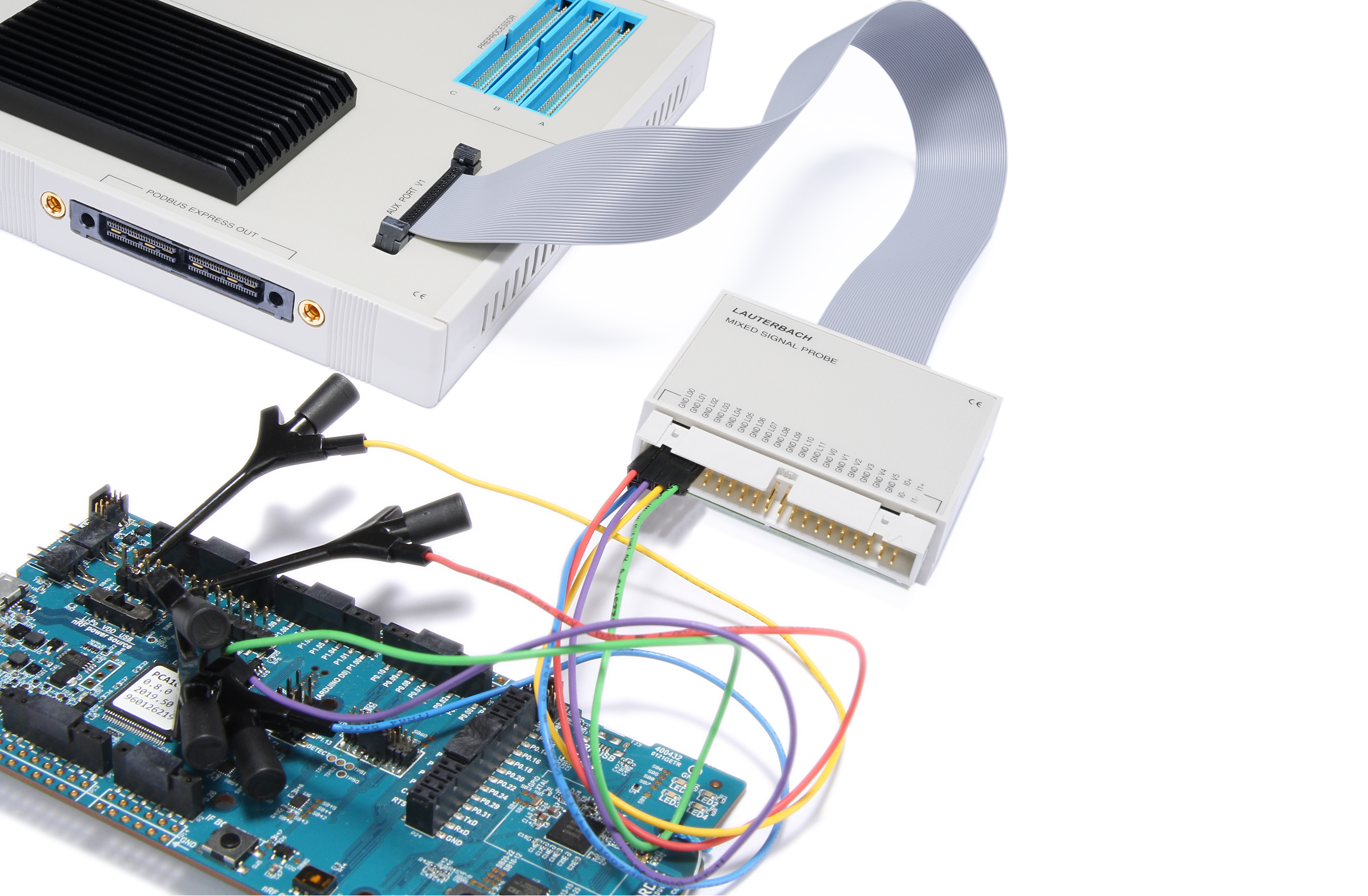
Our logic analyzers are the perfect extensions to our debug and trace tools. They allow the recording of digital and analog signals, which can be correlated to the recorded program flow. This way it is easy to verify signal-timings which are initiated by the application software or to calculate the power consumption of specific program parts.
TECHNICAL DATA
Compare Logic Analyzer Extensions
 |
 |
 |
|
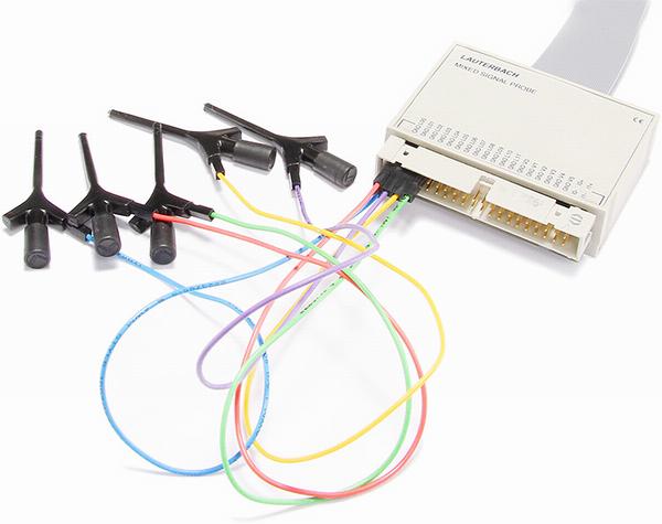
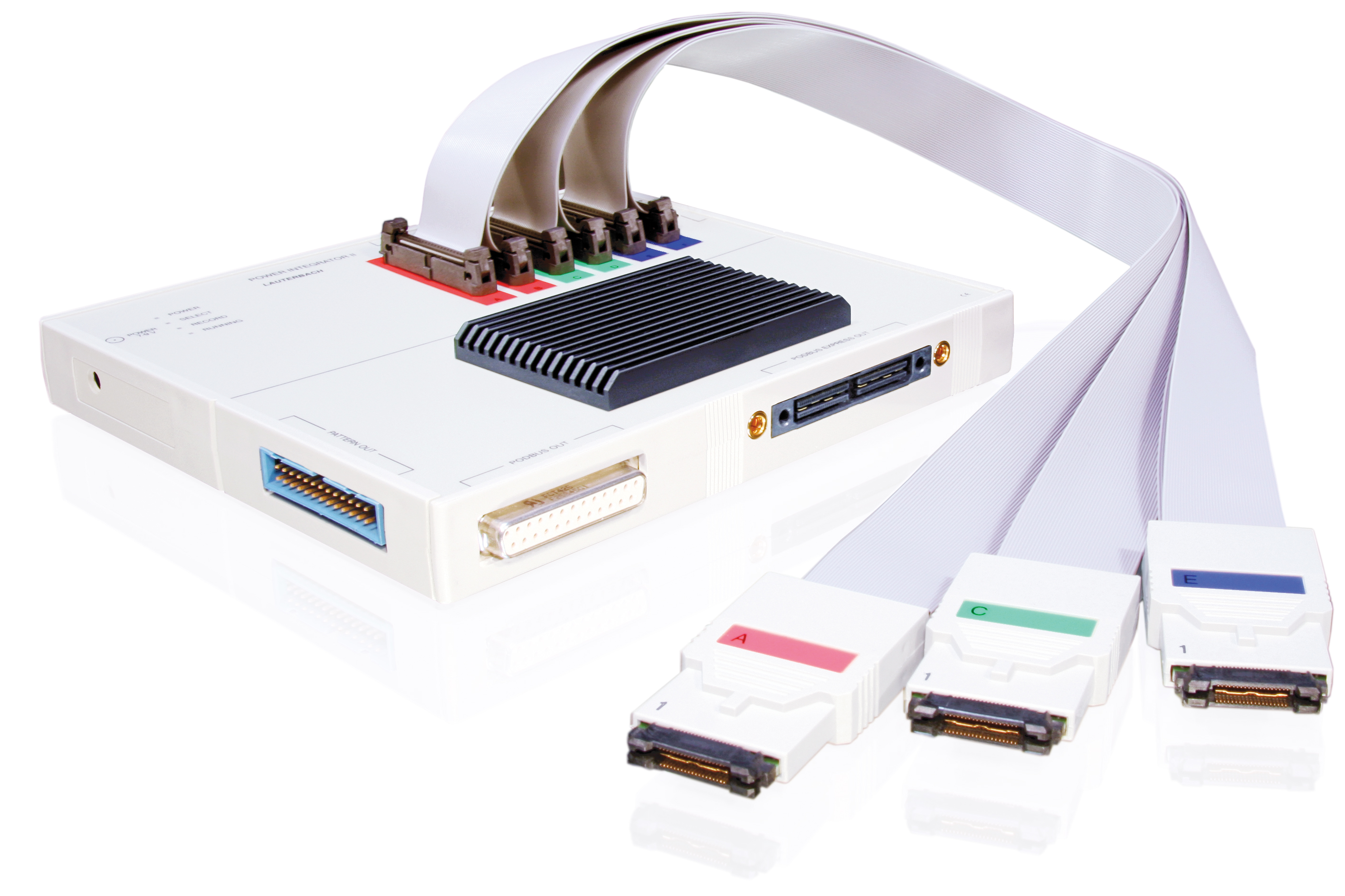
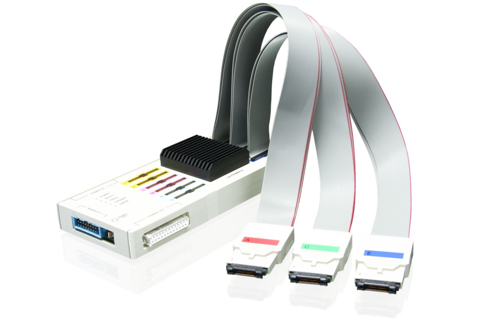
| Product | Mixed-Signal Probe | PowerIntegrator II | PowerIntegrator |
| Description | Allrounder (Most Popular) | Solution for extra long recordings of many signals | Solution for many signals or wide buses |
| Signal Type | Digital and Analog | Digital and Analog through specific probes | Digital and Analog through specific probes |
| Inputs | 12 digital channels, 6 single-ended voltage channels, 2 current measurements | Up to 102 digital channels, up to 8 signal ended voltage, up to 6 current measurements | Up to 204 digital channels, up to 8 signal ended voltage, up to 6 current measurements |
| Digital Input Voltage | 0-5V | 0-5V | 0-5V |
| Digital Threshold Voltage | 0.1V - 2.5V | 0.1V - 2.5V | 0.1V - 2.5V |
| Digital Sampling Rate | 200 MSamples/s per channel | 500 MSamples/s per channel | 500 MSamples/s per channel |
| Analog Input Voltage | -12V - +12V | 0V - +5V | 0V - +5V |
| Analog Resolution | 13 bit | 12 bit | 12 bit |
| Analog Sampling Rate | 1 MSample/s | 625 KSample/s | 625 KSample/s |
| Trigger Output | Not Available | 5 trigger outputs | Not Available |
| Compatible Modules | PowerTrace Serial 2, PowerTrace III, MicroTrace and CombiProbe 2 | PowerDebug II, PowerDebug PRO, PowerDebug X50/X51 | PowerDebug II, PowerDebug PRO, PowerDebug X50/X51, PowerDebug E40, PowerDebug USB 3.0 |
| Streaming Mode | Yes | Yes | No |