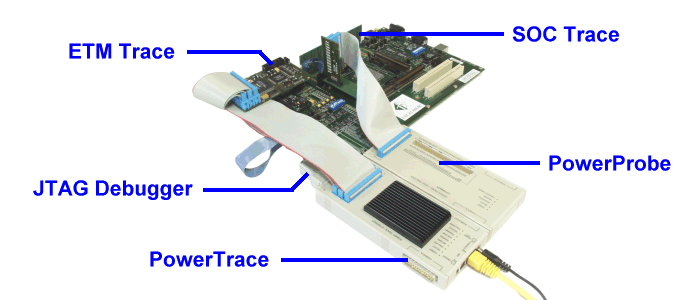
The ALTERA EXCALIBUR board can be adapted to 3 different tools The ALTERA EXCALIBUR board can be adapted to 3 different tools
|
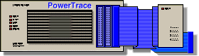
 PowerTrace PowerTrace
|
|
JTAG Debugger

|
- Multicore debugging
- Multiprocessor debugging
- Display of internal and external peripherals at a logical level
- Flash programming
- OS awareness debugging
- Powerful script language
|
|
ETM Trace for Program Flow and Core Data

|

- Up to 8 GByte trace buffer
- Target voltage 1.2 .. 3.3 V
- 5 ns time stamp
- Program and data trace
- Performance analysis
- Function and task run-time measurement
- AUTOSAR-aware profiling
- Code coverage
- Support for Embedded Trace Macrocell (ETM), Program Trace Macrocell (PTM)
- Support for Embedded Trace Buffer (ETB), Trace Memory Controller (TMC), Trace Port Interface Unit (TPIU)
- Support for multiple trace sources in a single stream (CoreSight trace)
|
|
PowerProbe

|
- Timing Analyzer up to 400 MHz
- State Analyzer up to 100 MHz
- 64 Input Channels
- Transient Recording
- Time Correlation with RISC Trace
- Clock Qualifier for State Clock
- Mixed State and Timing Mode
- 4 State Clock Inputs
- Optional FPGA Onchip Trace
- Optional Pattern Generator
- Protocol Support for CAN, USB, etc.
|
|
SOC-Trace for On-Chip Peripherals


|
Adapter for Excalibur Board
|
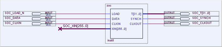
Step 1 Integration of SOC Scanner Module in Firmware
The SOC scanner is integrated on the top-level module and the trace and control lines
are connected to X123:
	SOC_T[0]     : LOCATION = Pin_N11;
	SOC_T[1]     : LOCATION = Pin_AH11;
	SOC_T[2]     : LOCATION = Pin_N12;
	SOC_T[3]     : LOCATION = Pin_AC12;
	SOC_T[4]     : LOCATION = Pin_N13;
	SOC_T[5]     : LOCATION = Pin_AE11;
	SOC_T[6]     : LOCATION = Pin_M5;
	SOC_T[7]     : LOCATION = Pin_AB12;
	SOC_T[8]     : LOCATION = Pin_L5;
	SOC_T[9]     : LOCATION = Pin_AD11;
	SOC_T[10]    : LOCATION = Pin_K4;
	SOC_T[11]    : LOCATION = Pin_A8;
	SOC_T[12]    : LOCATION = Pin_E6;
	SOC_T[13]    : LOCATION = Pin_J4;
	SOC_T[14]    : LOCATION = Pin_E7;
	SOC_T[15]    : LOCATION = Pin_H4;
	SOC_T[16]    : LOCATION = Pin_C8;
	SOC_T[17]    : LOCATION = Pin_K5;
	SOC_T[18]    : LOCATION = Pin_B8;
	SOC_T[19]    : LOCATION = Pin_E4;
	SOC_T[20]    : LOCATION = Pin_E9;
	SOC_T[21]    : LOCATION = Pin_J5;
	SOC_T[22]    : LOCATION = Pin_E8;
	SOC_T[23]    : LOCATION = Pin_H5;
	SOC_T[24]    : LOCATION = Pin_D8;
	SOC_T[25]    : LOCATION = Pin_G5;
	SOC_T[26]    : LOCATION = Pin_B5;
	SOC_T[27]    : LOCATION = Pin_F5;
	SOC_T[28]    : LOCATION = Pin_A5;
	SOC_T[29]    : LOCATION = Pin_E5;
	SOC_T[30]    : LOCATION = Pin_E10;
	SOC_T[31]    : LOCATION = Pin_D5;
	SOC_CLKIN    : LOCATION = Pin_AD12;
	SOC_CLKOUT   : LOCATION = Pin_N4;
	SOC_SYNCH    : LOCATION = Pin_AF11;
	SOC_LOAD_N   : LOCATION = Pin_P13;
	SOC_DATA     : LOCATION = Pin_P4;
Step 2 Connection via Adapter to EXCALIBUR board
Step 3 Defining signal names for SOC Trace
      PP::
      NAME.RESET
      NAME.SET x.0 USER_LED0
      NAME.SET x.1 USER_LED1
      NAME.SET x.2 USER_LED2
      NAME.SET x.3 USER_LED3
      NAME.SET x.0 USER_LED4
      NAME.SET x.1 USER_LED5
      NAME.SET x.2 USER_LED6
      NAME.SET x.3 USER_LED7
Step 4 Operation Settings
    ANALYZER.CSELECT USER_LED0
    ANALYZER.CSELECT USER_LED1
    ANALYZER.CSELECT USER_LED2
    ANALYZER.CSELECT USER_LED3
    ANALYZER.CSELECT USER_LED4
    ANALYZER.CSELECT USER_LED5
    ANALYZER.CSELECT USER_LED6
    ANALYZER.CSELECT USER_LED7

    ANALYZER.MODE 8X32

    ANALYZER.RATE TRANSIENT

    ANALYZER.MODE 100MHZ
Step 5 Project Compilation and Loading
An example design 'Hello' shows typical use of the SOC module, to trace the internal signals in FPGA device using
PowerProbe device. The example has been compiled using Quartus software and GNU compiler. File 'Hello.zip' contains a
complete project for Quartus software and all necessary source and design files.
The compilation process will produce an hex file 'hello_flash.hex' used to program on-board boot flash devices. This
file must be programmed into on-board flash memory devices on Excalibur evaluation board, using ByteBlaster cable and
'exc_flash_programmer.exe' utility, delivered with Quartus software.
The inputs/outputs of the embedded SOC block in Excalibur device have been mapped on the pins bounded to EPXA10
development board expansion connector U123. An special adapter MEPG-1 lets to connect SOC trace adapter MEPA-3
to the EPXA10 board using an Mictor connector.
A Practice file 'hello_demo.cmm' sets a appropriate configuration for SOC block.
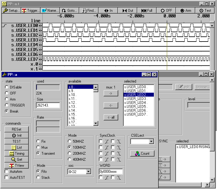
Step 6 Display
| 

 Adaptation for Excalibur
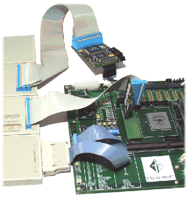


 [www.altera.com] Altera Excalibur Site
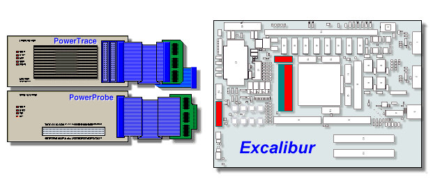
 ARM/Cortex Trace (parallel)