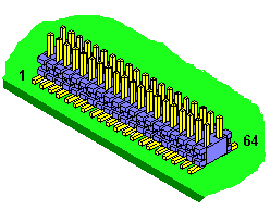
Universal EPROM/Flash Adapter |
 |
|||||

|
||||||
| ||||||
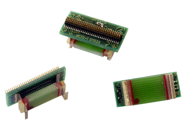
 Target Adaptation for EPROM/FLASH Simulator
|
 |
| ||||||||||

 The ESI-CON is an universal connector for embedded targets using 8 or 16 bit FLASH or EPROM devices. The connector includes following functions:
| ||||||||||||||||||||||||||||||||||||||||||||||||||||||||||||||||||||||||||||||||||||||||||||||||||||||||||||||||||||||||||||||||||||||||||||||||||||||||||||||||||||||||||||||||||||||||||||||||||||||||||||||||||||||||||||||||||||||||||||||||||||||||||||||||||||||||||||||||||||||||||||||||||||||||||||||||||||||||||||||||||||||||||||||||||||||||||||||||||||||||||||
 Application Note
| Connector | Pins | Function | Notes |
|---|---|---|---|
 |
40 | 8 Bit EPROM/FLASH Simulation and ROM monitor function without RESET and NMI control | |
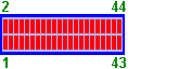 |
44 | 8 Bit EPROM/FLASH Simulation and ROM monitor function with RESET and NMI control | |
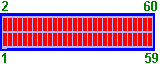 |
60 | 8/16 Bit EPROM/FLASH Simulation and ROM monitor function with RESET and NMI control | |
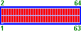 |
64 | 8/16 Bit EPROM/FLASH Simulation and ROM monitor function with RESET and NMI control, and automatic voltage control |
 Connector Orientation
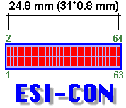
| Signal | Pin | Pin | Signal | ||
|---|---|---|---|---|---|
 | |||||
| GND | 1 |  |  | 2 | GND |
| A11 | 3 | | | 4 | A12 |
| A10 | 5 | | | 6 | A13 |
| A09 | 7 | | | 8 | A14 |
| A08 | 9 | | | 10 | A15 |
| A07 | 11 | | | 12 | A16 |
| A06 | 13 | | | 14 | A17 |
| A05 | 15 | | | 16 | A18 |
| A04 | 17 | | | 18 | A19 |
| A03 | 19 | | | 20 | A20 |
| A02 | 21 | | | 22 | A21 |
| A01 | 23 | | | 24 | A22 |
| A00 | 25 | | | 26 | A23 |
| (OPFETCH-)* | 27 | | | 28 | (WRITE-)* |
| CE_LOWERBYTE- | 29 | | | 30 | OE_LOWERBYTE- |
| D00 | 31 | | | 32 | D01 |
| D02 | 33 | | | 34 | D03 |
| D04 | 35 | | | 36 | D05 |
| D06 | 37 | | | 38 | D07 |
| GND | 39 | | | 40 | VCC_TARGET |
| GNDS | 41 | | | 42 | RESET+/- |
| VCCS | 43 | | | 44 | NMI+/- |
| WORD_SELECT- | 45 | | | 46 | (CYCLE-)* |
| GND | 47 | | | 48 | GND |
| CE_UPPERBYTE- | 49 | | | 50 | OE_UPPERBYTE- |
| D08 | 51 | | | 52 | D09 |
| D10 | 53 | | | 54 | D11 |
| D12 | 55 | | | 56 | D13 |
| D14 | 57 | | | 58 | D15 |
| GND | 59 | | | 60 | GND |
| VCC_BUFFER | 61 | | | 62 | VCC_3VOLT |
| VCC_INTERN | 63 | | | 64 | VCC_TARGET |
 | |||||
|
||||||||||||||||||||||||||||||||||||||||||||||||||||||||||||||||||||||||||||||||||||||||||||||||||||||||||||||||||||||||||||||
| ||||||||||||||||||||||||||||||||||||||||||||||||||||||||||||||||||||||||||||||||||||||||||||||||||||||||||||||||||||||||||||||


|
Copyright © 2024 Lauterbach GmbH, Altlaufstr.40, 85635 Höhenkirchen-Siegertsbrunn, Germany
Impressum
Privacy Policy
The information presented is intended to give overview information only. Changes and technical enhancements or modifications can be made without notice. Report Errors Last generated/modified: 07-Mar-2024 |
